

Semiconductor Manufacturing Equipment Market Growth Analysis Research Report By Product Type: Logic Devices, Memory Devices, Analog Devices, Optoelectronics, Sensors, Others, By Application: Foundry & Logic Manufacturing, DRAM Manufacturing, NAND Manufacturing, Analog & Mixed Signal Devices, Discrete Devices, Optoelectronics, By Dimension (Integration Technology): 2D ICs, 2.5D ICs, 3D ICs - and Global Forecast to 2034
Feb-2026 Formats | PDF | Category: Electronics & Semiconductor | Delivery: 24 to 72 Hours
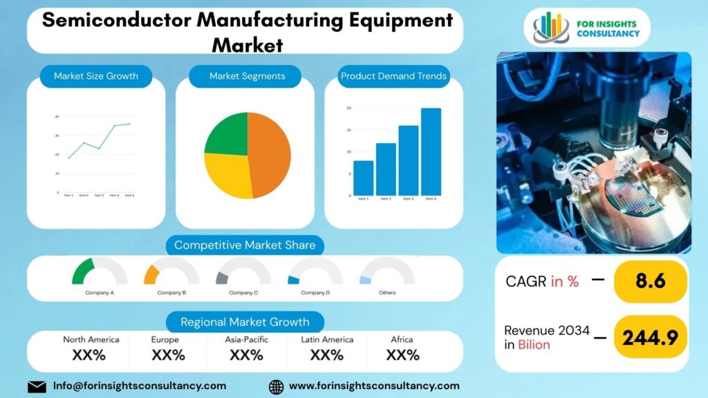
The Global Semiconductor Manufacturing Equipment Market is expected to be valued at USD 13.4 Billion in 2025 and is anticipated to reach USD 244.9 Billion by 2034, growing at a compound annual growth rate (CAGR) of 8.6% from 2026 to 2034.
Semiconductor Manufacturing Equipment Market: Overview and Growth in the Upcoming Year
The growth in the Semiconductor Manufacturing Equipment market in the coming year reflects the growth in semiconductor manufacturing needed to meet the growing demand for manufactured semiconductors across the globe. Ongoing construction of additional chip production facilities also supports this growth. In the current climate of widespread digital transformation in all business ecosystems, semiconductor manufacturers are being selective in the areas of efficiency, precision, and technological advancement (including Artificial Intelligence, High-Performance Computing, Electric Vehicles, and Advanced Communicative Infrastructure) and are therefore increasing their capital investments.
A more precise outlook for 2026 shows the demand for more advanced and increased wafer production capacity. In the area of smaller and more advanced packaging of semiconductors, integrated device manufacturers and foundries are more likely to shift to and invest in the more energy efficient and high-performance semiconductors. In this area of manufacturing lithography, deposition, etching, and inspection systems will continue to receive intensive investments with an overall manufacturing focus.
How does Government Investment Impact the Semiconductor Manufacturing Industry?
Government investment in the fabrication equipment sector is occurring due to the number of fabrication plants currently being built and planned to be built in the coming years. The number of plants under construction is indicative of the investment being made in the fabrication equipment sector. Increasing government investment encourages both remaining and new stakeholders to introduce innovative production technologies. These government investments in fabrication plants directly correlate to the investments being made by Wafer Manufacturing Equipment (WFE) and Advanced Packaging Equipment (APE) fabrication plants.
The investments made by governments in fabrication plants open new markets for other vendors to provide equipment and fabrication plants flexible in terms of the equipment provided. So going forward, investment in government plants as they correlate to private investment in the Equipment and WFE and APE fabrication plants are where the governments’ and private sector’s investments in the plants will meet. It can be assumed there will be a significant number of plants to provide flexible (custom) fabrication equipment, and to meet the increasing demand for substrates and other equipment and products.
The long-term outlook for the Semiconductor Manufacturing Equipment (SME) industry remains positive due to the SME sector’s quality of long-term investment. The Semiconductor Manufacturing Equipment sector is characterized by a high level of automation, complex data, and the ability to give factory data.
Advanced Automation Technology (AAT) and Artificial Intelligence (AI) are deployed in the SME sector to increase yield and quality, and minimize downtime. Technology (AI) is used to increase the operational reliability of the manufacturing equipment and to provide the necessary environment for modern chip makers to manufacture the ever increasingly complex chips.
From now until 2026, growth in the Semiconductor Manufacturing Equipment industry is expected to remain steady, rather than driven by short-term growth. Although there is an industry cycle that is unavoidable within semiconductor manufacturing, there are many long-term reasons to continue investing in equipment.
These reasons include the growth of cloud computing and the IoT, the electrification of vehicles, and advanced consumer electronics. Therefore, the market will also continue making investments in automation, advanced node manufacturing, and innovative growth, demonstrating the importance of the market to the global technological value chain.
Market Dynamics
Growth Drivers
Grown Need for Sophisticated Semiconductors.
The continuing adoption of artificial intelligence, high-performance computing and smart consumer electronics is saturating the chipmakers fabrication capacity, which increases the demand from manufacturing equipment.
Growth of global semiconductor manufacturing plants.
New wafer fabrication plants are being developed at a rapid pace in major semiconductor-producing regions which have created a sustained demand for lithography, deposition, etching, and inspection systems.
Move to high development processes.
The move to smaller nanometer technologies requires more sophisticated and accurate equipment which forces continuous upgrades and replacements within a fabrication facility.
Surge of Electric Cars and Automotive Electronics.
Advanced driver-assistance systems (ADAS), along with other in-vehicle electrochemical large batteries, connected vehicles and electric powertrains, have gained significant traction in recent years.
Restraints
Substantial Required Financial Commitment
Due to the large initial costs associated with semiconductor fabrication equipment, small manufacturers and potential entrants into the market find it difficult to obtain funding for expansion projects.
Semiconductor Market’s Cyclical Characteristics
Due to the cyclical nature of semiconductor production, market demands for semiconductor equipment is equally cyclical, resulting in an equipment purchase freeze during an excess supply and low demand for chips.
Difficulties with the Development and Integration of Technologies
The advanced tools of semiconductor manufacturing are, heightened operational complexities and elongated periods for the use of the tools from innovating the tools in their entirety.
Critical component supply chain disruptions
Logistical or geopolitical disruptions in global supply chains can lead to delays in production for materials of low, precision optics, and specialized electronics.
Opportunities
Integration of AI and High-Performance Computing
The rapid integration of AI across numerous sectors and the advancements in computing technology represent substantial opportunities for suppliers providing next-generation chip architectures with extremely precise fabrication needs.
Advancements of the AI Pack and Heterogeneous Integration
The rapid adoption of AI packs and heterogeneous integration technologies creates opportunities for assembly, bonding, and inspection equipment focused on next-generation packaging.
The Shift of Semiconductor Manufacturing to the Domestic Location
The shift to home-region domestic semiconductor ecosystems creates opportunities for partnerships, service center, and supply agreements for manufacturers.
Increase in Automotive and Power Semiconductors
The rise in electric vehicles, and sophisticated autonomous driving systems, along with power electronics, have increased the demand for tailored automotive-grade chips, thereby requiring specialized equipment for wafer fabrication and testing.
Challenges
Growing Complexity of Advanced Nodes
Designing chips at smaller nanometer scales involves higher intricacies and multi-step processes that require more precision, more advanced technologies, and more costly equipment to manufacture.
Unpredictable Cycles of Semiconductor Demand
Demand for consumer electronics, memory pricing, and global spending on technology fluctuate and creates unpredictable patterns in equipment ordering, suppliers find it more difficult to plan their production.
Lengthy Qualification of Equipment to be used in Manufacturing
A notoriously lengthy process for semiconductor fabs is tool-testing and tool-qualification, and this stagnation tends to push revenue capture for tool manufacturers even further into the future.
Soaring Research and Development Costs
To stay relevant in the marketplace, the pressures are on companies to spend more on research and development, and this burdens mid-tier manufacturers in the equipment sector the most.
Top Companies Covered In This Report
- Applied Materials Inc.
- Lam Research Corporation
- KLA Corporation
- ASML
- Tokyo Electron Limited
- Advantest Corporation
- SCREEN Semiconductor Solutions Co., Ltd.
- Cohu, Inc.
- ACM Research Inc.
- Nordson Corporation
- Tokyo Seimitsu Co., Ltd.
- EV Group (EVG)
- Modutek Corporation
- Dainippon Screen Group
- Ferrotec Holdings Corporation
Semiconductor Manufacturing Equipment Industry Company News
Applied Materials Inc.
News (2025-2026): Reported strong momentum entering 2026, expecting over 20% growth in semiconductor equipment driven by AI computing, advanced logic, and high-bandwidth memory demand. Expanded focus on advanced packaging and hybrid bonding technologies supporting next-generation chip architectures.
Industry impact:
Applied Materials’ investments reinforce the shift toward AI-optimized fabrication and advanced packaging, accelerating capital spending cycles while also emphasizing regulatory risk management across global supply chains.
Lam Research Corporation
News (2025–2026):
Achieved important customer wins for advanced etch systems supporting 3D DRAM and next-generation memory production. Benefited from rising demand for DDR5 and high-bandwidth memory manufacturing transitions.
Industry impact:
Lam Research strengthens the etch equipment segment, enabling memory scaling and reinforcing the growing equipment intensity per wafer as chip architectures become more complex.
Tokyo Electron Limited
2026 Focus:
Expanded involvement in advanced packaging and wafer processing technologies alongside global equipment peers.
Industry impact:
Tokyo Electron’s expansion supports the industry’s transition from traditional scaling toward heterogeneous integration and packaging innovation.
Cohu, Inc.
Company News (2025–2026):
Focused on semiconductor test handling and automation solutions aligned with automotive and industrial chip reliability requirements.
Industry Impact
Growing automotive semiconductor standards are expanding long-term demand for reliability testing and automated inspection systems.
Detailed Segmentation and Classification of the report (Market Size and Forecast – 2034, Y-o-Y growth rate, and CAGR):
Segment By Product Type
- Logic Devices
- Memory Devices
- Analog Devices
- Optoelectronics
- Sensors
- Others
Segment by Application
- Foundry & Logic Manufacturing
- DRAM Manufacturing
- NAND Manufacturing
- Analog & Mixed Signal Devices
- Discrete Devices
- Optoelectronics
Segment by Dimension (Integration Technology):
- 2D ICs
- 5D ICs
- 3D ICs
Segment by End User
- Semiconductor Foundry
- Integrated Device Manufacturers (IDMs)
- Outsourced Semiconductor Assembly & Test (OSAT) Providers
- Research Institutes & Pilot Lines
Segment by Manufacturing Facility Size
- Large-Scale Manufacturing Facilities
- Medium-Scale Manufacturing Facilities
- Small-Scale Manufacturing Facilities
Segment bySupply Chain Process
- Wafer Fabrication
- Assembly & Packaging
- Testing & Inspection
Regional Deep-dive Analysis:
The report provides in-depth qualitative and quantitative data on the Semiconductor Manufacturing Equipment Market for all of the regions and countries listed below:
North America
North America keeps pivotal importance in semiconductor manufacturing especially in the years to come because of many developing technology, government funding, and fabrication plants. Manufacturing plants in this area have a well developed and established ecosystem to make semiconductors including varied and developed manufacturing directed research and development, a workforce, and technology in high-end processing.
Utilization of the U.S. Fab Expansion
In the U.S. construction of various logic and memory manipulation plants are taking place in the states Arizona, Texas and New York, these plants are meant to implement the most modern manufacturing.
Incentives by the Government. Stimuli programs made by the CHIPS Act in the U.S. support the production of domestic chips which in turn creates the need of construction of wafer fabrication and testing plants.
Focus on Advanced Other Back End Packaging. Due to the recent high backing demand for equipment, the use of the 2.5D and 3D packaging has increased in chips related to artificial intelligence, high performance computing, and automotive.
Innovation and Research and Development. The presence of well and great institutions of the developing semiconductor and the research centers increases the demand for the latest developed semiconductor tools such as lithography, deposition, and metrology.
Supply Chain Resilience. In North America, priority becomes regionally supported and diversified sources for equipment to retake services to support the equipment globally.
Canada
With the development of sensors, quantum computing chips, and niche analog devices, small scale equipment demand becomes great.
With the Research and Pilot Lines. Once the production of tester and inspection equipment becomes established, Canadian universities and research centers will have the opportunity to construct pilot production lines, thus advancing the production of these devices greatly.
Government Assistance: Fiscal policies assisting innovation in semiconductor manufacturing increase initial adoption of cutting-edge fabrication tools.
Mexico
Assembly & Packaging Center: Mexico continues to position itself as an expanding site for outsourced assembly and packaging (OSAT), increasing demand for back-end and testing tools.
Workforce Cost Benefits: Manufacturing labor that is less expensive promotes the establishment of mid-scale assembly and wafer testing facilities.
Transnational Cooperation: Robust relations with the U.S. simplify the transport of equipment and service integration.
Europe
In 2026, Europe will remain strategically important in the semiconductor manufacturing equipment market. The region specializes in research and development for advanced semiconductors, specialty chips, and fab modernization. European self-sufficiency is improving as the EU has been rolling multiple programs, including a semiconductor directive and incentives for domestic chips.
Germany
Germany allocates more than 5 billion euros. It will go to semiconductor foundries that manufacture logic chips and HPC.
Germany, the automobile’s core, will be a major beneficiary. That is, more demand for automotive semiconductor manufacturing equipment. For example, it may likely be for electric vehicles. Also, more demand for advanced packaging and wafer testing equipment.
A good number of research institutions and corporate R&D centres accelerate the adoption of next-generation lithography, etch and deposition tools.
France
Specialty Semiconductors focuses on analog, mixed-signal devices, and sensors for industrial and auto applications.
France is financing the production of pilot lines with government grants that create demand for small- to mid-scale fabrication and testing equipment.
Funding Programs: They encourage the deployment of efficient and precision equipment in regional fabs.
Netherland.
Having many lithography equipment suppliers, they are encouraging EUV adoption across European fabs.
Cutting-Edge Node Investment: Dutch fabs play a central role in the production of leading-edge logic chips, increasing demand for critical metrology, inspection and deposition tools.
Industry and university partnerships drive process innovation and adoption of advanced packaging.
Italy and Eastern Europe.
Italy, with Eastern European countries like Poland and Hungary, is rapidly becoming a location for OSAT and wafer-level packaging assembly and packaging functions.
Demands for Mid-Scale Equipment; Capacities in these areas focus on assembly testing and inspection equipment rather than advanced node front-end systems.
Competitive labor costs will drive growth of mid-cap semiconductor manufacturing by keeping quality at moderate levels.
Asia-Pacific
In the Asia-Pacific (APAC) regions, the demand from semiconductor manufacturing equipment is expected to rise, APAC is expected to dominate due to the government investments and incentives to wafer fabrication on a larger scale. The APAC semiconductor ecosystem has a large production volume and also has strong and rapid supply chains and the adoption for AI, Automotive, and consumer electronics end use applications.
The China region is seeing the largest rapid construction of fab that are large scale and incorporate logic, memory and specialty chips. The construction of such fabs is creating greater demands for construction of lithography, deposition, etch and testing systems. China has policies, subsidies and also encourages self sustaining semiconductor programs as part of their strategy for self sustaining infrastructure for advanced tools to be integrated.
The construction of advanced packaging systems will support and increase the need for back end equipment in the support of 2.5D and 3D chiplet as well as high bandwidth memory chip packaging. As the supply chain is localizing the importing of high tech equipment from international sources will also be reduced.
Taiwan is dominating the logic and memory production. The country has advanced node logic and memory chips and is the leader in the use of EUV lithography, deposition, etch and metrology systems. High levels of Capital are required for continuous technological changes, expansions and upgrades of TSMC advanced node Fabs as they require long term investment in equipment to ensure top production levels. The country has a strong engineering and research workforce that is to a greater extent able to integrate AI assisted automation in fabrication.
South Korea Memory Dominance
The demand for South Korea’s memory info tech sequencing goods is on the rise due to the location of South Korea’s Memory Dominance global leaders for DRAM and NAND memory technologies and the continued memory scaling technologies that South Korea provides.
Technology Modernization
As a result of the increasing need for South Korea to modernize its technologies with next-generation logic and DRAM nodes, South Korea is a global leader in the modernization of packaging and wafer fabrication tools.
Back-End Innovation
The new packaging systems that have been developed for High Performance Computing (HPC) and Artificial Intelligence (AI) accelerators are rapidly expanding the market for testing and assembly equipment.
Japan
Specialty and Mature-Node Focus
The growing demand for production equipment for analog, discrete, and sensor devices is fostering equipment growth on the middle and small scale for Japan and the Asia Pacific region.
Equipment Manufacturing Leadership
Japanese fabrication, cleaning, and etching, and wafer deposition tool manufacturers are global leaders in the supply of those tools for the semiconductor industry.
Pilot Lines and Research Initiatives
The work of the R&D departments of the universities and companies is vital to the production of advanced specialized semiconductors and the prototyping of those semiconductors with specialized equipment at the small scale.
Southeast Asia (Singapore, Malaysia, Thailand)
OSAT and Back-End Manufacturing Hub
Countries such as Malaysia and Singapore have become the main back-end assembly, testing, and packaging hubs in the region.
Mid-Scale Equipment Growth
The development of mid-scale equipment for wafer testing, bonding, and inspection systems is on the rise, particularly for automotive, IoT, and consumer electronics chips.
Skilled Workforce and Logistics
The efficient logistics and skilled labor in the countries also provides a competitive advantage in the back-end semiconductor processes.
Frequently Asked Questions with Answers
What is the Semiconductor Manufacturing Equipment market size and growth forecast?
Semiconductor Manufacturing Equipment Market is projected to reach a value of USD 13.4 Billion in 2025 and is anticipated to grow to approximately USD 244.9 billion by 2034. This expansion reflects a compound annual growth rate (CAGR) of 8.6% during the forecast period from 2026 to 2034.
Who are the key players in the Semiconductor Manufacturing Equipment market?
The Semiconductor Manufacturing Equipment Market Includes Major Companies Applied Materials Inc., Lam Research Corporation, KLA Corporation, ASML, Tokyo Electron Limited, Advantest Corporation, SCREEN Semiconductor Solutions Co., Ltd., Cohu, Inc., ACM Research Inc., Nordson Corporation, Tokyo Seimitsu Co., Ltd., EV Group (EVG), Modutek Corporation, Dainippon Screen Group, Ferrotec Holdings Corporation, Others.
What are the current and future trends for Semiconductor Manufacturing Equipment market?
The Semiconductor Manufacturing Equipment market is trending toward AI-driven chip production, advanced node miniaturization, heterogeneous and advanced packaging technologies, smart factory automation, and geographically diversified semiconductor manufacturing investments.
Which regions dominate the Semiconductor Manufacturing Equipment market?
The Asia-Pacific region dominates the Semiconductor Manufacturing Equipment market, led by strong semiconductor manufacturing activity in countries such as China, Taiwan, South Korea, and Japan.
Key insights provided by the report that could help you take critical strategic decisions?
- Regional reports analyse product/service consumption and market factors in each region.
- Reports highlight possibilities and dangers for suppliers in the Semiconductor Manufacturing Equipment Market business globally.
- The report identifies regions and sectors with the highest growth potential.
- It provides a competitive market ranking of major companies, as well as information on new product launches, partnerships, business expansions, and acquisitions.
- The report includes a comprehensive corporate profile with company overviews, insights, product benchmarks, and SWOT analysis for key market participants.
Customization: We can provide following things
1) On request more company profiles (competitors)
2) Data about particular country or region
3) We will incorporate the same with no additional cost (Post conducting feasibility).
Any Requirement Contact us: https://www.forinsightsconsultancy.com/contact-us/
Table of Contents
For TOC Contact us: https://forinsightsconsultancy.com/contact-us/